Integrated Silicon Photonic Switch Demonstrates Lowest Signal Loss Ever in High-Speed Data Transmission
Experimental photonic switches tested by researchers at the University of California, Berkeley, U.S.A., show promise toward the goal of fully optical, high-capacity switching for future high-speed data transmission networks. The switch developed and tested for this research demonstrated capabilities not seen before in photonic switches.
This press release features multimedia. View the full release here: https://www.businesswire.com/news/home/20190228005731/en/
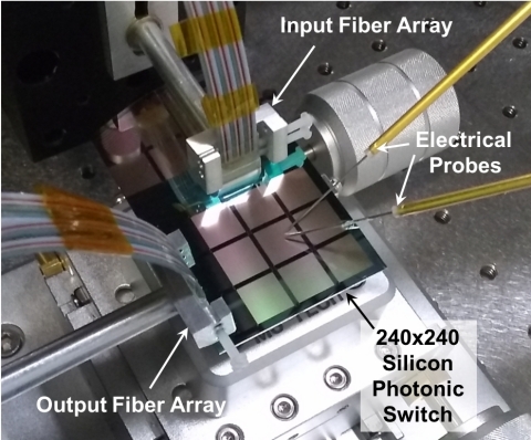
Photo of the fabricated 240x240 silicon photonic switch on the characterization setup. Credit: Tae Joon Seok
In a paper to be presented at OFC: The Optical Fiber Communications Conference and Exhibition, to be held 3-7 March in San Diego, Calif., U.S.A., researchers Tae Joon Seok and colleagues will report successful scale up of a 240x240 integrated silicon photonic switch. The device is so-named because it accepts 240 optical communication input channels and sends them into 240 output channels.
Using experimental photonic switches manufactured at the Marvell Nanofabrication Laboratory at UC Berkeley, the research team demonstrated signal loss lower than any previously reported, said Seok, who is assistant professor at the Gwangju Institute of Science and Technology in South Korea and a visiting scholar at UC Berkeley.
Addressing industry needs with advanced optical switching
The telecommunications industry long ago embraced fiber-optic technology as a better solution to meet exploding demand for higher speeds and greater capacity data transmission over the electrical copper wires of old. Now a similar revolution is occurring at the points where the messages transmitted over long-haul fibers are sent and received. Instead of power-hungry electrical switches that require optical-electrical-optical conversions and cause signal loss, researchers are developing and deploying photonic switches to improve transmission quality and link a single transmission to tens and sometimes thousands of servers.
In particular, silicon-based photonic switches using advanced complementary metal-oxide semi-conductor (CMOS) technology are drawing a lot of attention from researchers as a powerful platform due to their low cost and high capacity. They have the potential to replace electrical switches, which will soon face scalability limits in performance and energy efficiency. In order to realize this potential, researchers are now working to overcome limitations related to the size of today's silicon photonic chips and improve their performance.
"Recently, many research groups competitively reported silicon photonic switches with large input/output port counts," said Seok. However, the physical size of a silicon photonic chip has been limited to 2 to 3 cm because of the limitations of the lithography tools necessary to etch the required geometric patterns on the silicon wafers used as a base for the integrated chips.
Seok and his colleagues overcame this limitation by using a process known as lithography stitching, creating a wafer-scale 240x240 silicon photonic switch by stitching together nine 80x80 switch blocks in a 3x3 array, with three input and three output coupler blocks. The switches developed as part of the experiment coupled light coming in and out of the chip through grating couplers. The switch cells were actuated by electrical probes.
The resulting switch area was 4 cm x 4 cm—nearly doubling the size of existing silicon photonic switches. "To the best of our knowledge, this is the largest integrated photonic switch ever reported on any platform," Seok said.
Measured results from the experimental switch also broke records. "The on-chip loss to port-count ratio (0.04 dB/port) is the lowest demonstrated," Seok added.
"This technology can be applied not only to silicon photonic switches but also to any silicon photonics applications that require ultra-large-scale devices such as programmable photonic processors, and so on," Seok said.
Hear from the research team: “240x240 Wafer-Scale Silicon Photonic Switches” by Tae Joon Seok, Kyungmok Kwon, Johannes Henriksson, Jianheng Luo, Ming C. Wu will take place at 9:30 a.m. on Thursday, 7 March in Room 6D of the San Diego Convention Center.
MEDIA REGISTRATION: Media/analyst registration for OFC 2019 can be accessed online. Further information is available on the event website at OFC, including travel details.
About OFC
The Optical Fiber Conference and Exhibition (OFC) is the largest global conference and exhibition for optical communications and networking professionals. For more than 40 years, OFC has drawn attendees from all corners of the globe to meet and greet, teach and learn, make connections and move business forward.
OFC includes dynamic business programming, an exhibition of more than 700 companies, and high impact peer-reviewed research that, combined, showcase the trends and pulse of the entire optical networking and communications industry. OFC is managed by The Optical Society (OSA) and co-sponsored by OSA, the IEEE Communications Society (IEEE/ComSoc), and the IEEE Photonics Society. OFC 2019 will be held from 3-7 March 2019 at the San Diego Convention Center, California, USA. Follow @OFCConference, learn more at OFC Community LinkedIn, and watch highlights on OFC YouTube.
View source version on businesswire.com: https://www.businesswire.com/news/home/20190228005731/en/