Ultra-Precise Additive Printing for Flat Panel Display Manufacturing
The display sector faces some challenges: the progressive complexity of displays occurring with a reduced feature size, constant miniaturization, which causes yield issues on advanced manufacturing lines, expensive, complex, limited & slow yield improvement (repair) methods, and a need for the mechanical flexibility of new generation displays or electrical field damage risk - to name some of them. XTPL plans to support manufacturers in overcoming those issues by providing an additive, ultra-precise method that allows them to obtain conductive & non-conductive structures on the individual micron scale (1-8 μm).
This press release features multimedia. View the full release here: https://www.businesswire.com/news/home/20190509005596/en/
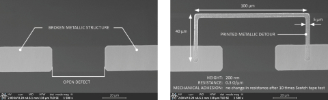
XTPL has developed an advanced additive method for open defect repair (ODR), strongly contributing to the increase of the production yield, that responds to manufacturers requirements. (Photo: Business Wire)
“We want to empower global electronics manufacturers by implementing our solution on their production lines. The XTPL vision entails using the traditional advantages of print - such as scalability, lower cost, simplicity and speed - in the production of advanced, high tech devices. Our technology responds to the market need of progressing miniaturization and at the same time provides a cost-effective & scalable method. We believe that as easily and inexpensively as you print books and newspapers today, soon you'll be able to print display, semiconductor or smart glass elements. The highest precision, one that will allow for this process to materialize, is what XTPL brings to the table.” – explains Filip Granek, CEO of XTPL
Unparalleled versatility
The XTPL disruptive solution works on most substrates, conductive and non-conductive, as well as flat and 2.5D, such as glass, silicon wafers, kapton, PEN, PC, PDMS, PET. It can provide straight lines, as well as patterns and microdots. This XTPL method allows the printing of a large variety of available materials: conductive inks, nanoparticle based suspensions, semiconductor based suspensions, insulating inks, resists, solvent based inks and biological materials. In order to achieve outstanding results, the company creates its own nanoink formulas based mostly on metallic nanoparticles (Ag, Au and Cu) and semiconductors (TiO2). There is no electric field required for printing, which fully eliminates the risk of damage to the substrate and other electrically active components. Parameters & features of individual structures created with this method, as well as the distance between them, depend on the specific application requirements.
XTPL solutions for nanoprinting may be applied in many sectors, mostly within printed electronics, e.g. in semiconductors, smart glass, advanced PCBs, anticounterfeiting or biosensors sector. The company’s key focus at the moment is the flat panel display market, where this technology provider has already verified serious competitive advantages.
Value for manufacturers
The feature size of printed structures is one of the key parameters when comparing additive technologies. The XTPL solution can provide structures on the individual micron scale (1-8 μm), which enables a higher pixel density of the finished products. In particular the resolution, brightness and lifetime parameters of the final display are improved.
Another challenge faced by the modern FPD manufacturing lies in the fact that ultra-fine conductive structures are prone to damage. This is a major factor contributing to the decrease of the production yield. The XTPL advanced additive method for open defect repair (ODR) responds to manufacturers requirements in this respect. It requires no electric field for printing, thus fully eliminating the risk of damage to the substrate and other electrically active components (non-electrostatic alternative to the EHD technology). Furthermore, it allows for the repair of broken conductive lines already at the production stage, which contributes to reduced takt time. The XTPL method is effective and enables the high spatial density of printed features, high adhesion to the substrate (various options possible), and all with a lower production cost for the manufacturers and no toxic substances used in the repair process.
Currently a strong trend for producers who aim to meet customers’ expectations is the introduction of flexible displays. Due to the high production costs and low yield of flexible electronics, its introduction on a mass scale proves to be a challenge. The XTPL solution enables the mechanical flexibility of new generation displays because electrically conductive structures obtained using this method retain their properties - including excellent electrical conductivity parameters - throughout the deformation of the substrate.
It is also worth mentioning that due to the highest transparency of XTPL structures and above mentioned excellent electrical conductivity parameters, as well as mechanical flexibility, this solution can potentially be applied as an alternative also in transparent metal mesh manufacturing.
XTPL technology can be potentially used in the future in OLED manufacturing to precisely deposit organic materials. Unlike the currently used fine metal mask (FMM) approach, structures obtained with our printing method do not exhibit a shadowing effect with the increase of display size. This advance allows for a reduced feature size, irrespective of the scaling. Since the XTPL solution is purely additive, no organic material is wasted and there is no need for masks that have to be replaced between the deposition cycles. Currently used state-of-the-art ink-jet printers for the OLED industry deposit structures with a minimal diameter of 20 μm, while XTPL technology provides microdots as small as 1 μm in diameter. Additionally, the implemented XTPL ultra-precise deposition (UPD) allows for the obtainment of arbitrary shapes on any kind of substrate currently used in OLEDs. The technology is also well suited for Colour Filter (C/F) deposition during the manufacture or repair stages of the OLED and LCD panel production process. Universality here allows for the deposition of a wide range of possible C/F materials, as well as sizes, and does not require any masking.
Meet XTPL at Display Week
“We are open to collaboration with display equipment manufacturers as well as display manufacturers themselves, to provide for them a high performance solution dedicated for industrial implementation. Hopefully we will be able to connect to the main players from this sector at the upcoming Display Week exhibition 14-16 May in San Jose at XTPL booth (number 431).” – invites Filip Granek
View source version on businesswire.com: https://www.businesswire.com/news/home/20190509005596/en/