Categories
- Electrical, Electronics & Electro-optics
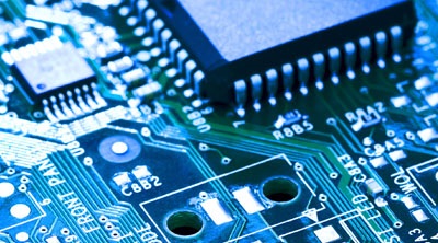
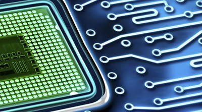
PCB Technologies Ltd. is a one-stop solution fabrication of high reliability, multilayer Printed Circuit Boards and top level assemblies (PCBA). Since 1981 the Company provides a wide range of manufacturing solutions that meet the highest industry standards. PCB Technologies' focus is serving highly demanding markets such as: Defense, Aerospace, Medical, RF/Microwave, Telecom and more. The Company's highly-experienced staff, state-of-the-art technologies and advanced processes help deliver innovative solutions and ensure cost-effective fabrication of the most challenging and complex boards.
PCB Technologies is a subsidiary of PriorTech Group and is traded on the Tel-Aviv Stock Exchange (symbol. PCBT). The company currently occupies 17,000 square meter in an advanced manufcaturing facility and employs a staff of 700 with an annual turnover of around $100 million. PCB Technologies' one-stop-shop for CEM services – from design to complete production, including full turnkey capabilities. In addition, the Company offers a complete line of bare board and assembled-board testing facilities, including in-circuit test (ICT), J-Tag, functional test and customized testing.
PCB Technologies' competitive advantages include:
- PWB Manufacturing and Assembly under one roof
- Highly experienced and creative engineering team
- Superior technical customer support
- Reputation for providing high-quality products to
- military and commercial markets
- Flexible operation with quick response time.
- Ability to handle low, mid, and high-volume runs
- Strong financial backing for future expansion
- Affiliated with the Prior-Tech Group, specializing in electronic packaging, development and production.

Assembly Services
PCB Technologies takes overall product responsibility from any point of design to complete production.
With their turnkey solutions, manufacturers can reduce logistics and inventory management costs and increase the availability of stock room space for R&D and other activities.
PCB Technologies offers an array of services including:
- In-house manufacturing of prototype, pilot and first production runs
- Material sourcing and purchasing
- New Product Introduction (NPI) services
- DFM for NPI
- Process validation
- Quick turnaround for engineering approval
- Wide range of testing capacities
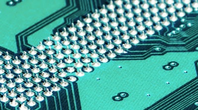
- SMD and TH technology
- BGA, Ceramic BGA and Micro BGA capability
- Press fit connectors
- ICT & Functional testing
- J-Tag testing
- BGA rework capability includes - Re-Balling of BGA components
- 3D X-Ray for BGA quality
- Mechanical assembly (boxes, harnesses, cables)
Assembly Special Services
- Design, Engineering, and E.C.O Support
- SMT, 6 lines
- Wave Soldering
- Press fit connectors insertion machine
- BGA, Ceramic BGA and Micro BGA capability
- BGA rework and Inspection capability
- Re-Balling of BGA components
- ROHS compliance
- Mechanical assembly (including boxes, harnesses, cables)
- ICT, J-Tag, Functional testing and testability design support
- 3D X-Ray for BGA quality
- ICT Fixture development and programming
- ESS and Burn-in
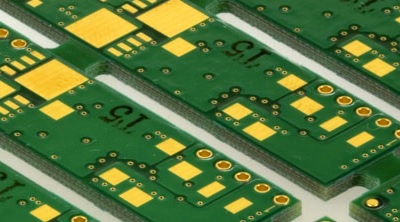
Multilayer Rigid, Rigid-Flex and Multi-Flex
PCB Technologies' PWB division specializes in the manufacture of a wide range of board types. The emphasis on R&D has helped the Company become a market leader in the development and manufacturing of advanced PWBs.
PCB Technologies capabilities include:
- Rigid boards up to 42 layers
- Flex and Rigid-Flex boards up to 40 layers
- Hybrid solutions for Microwave/RF applications
- Thermal and signal integrity management solutions, employing coins and cavities
- 2D or 3D heat-sinks: Copper and Aluminum
- Carbon printing
- HDI – blind, buried, staggered & stacked vias
- Buried passive components: capacitors and resistors
- In-house HATS lab

Materials
PCB Technologies works and partners with world-class qualified suppliers that use the best materials available for printed circuit board (PCB) manufacturing. The Company's detailed and comprehensive material inspection process ensures that suppliers comply with all requirements for satisfying customer needs.
Materials used by the Company include:
- Glass epoxy (GF) laminate, Tg - 180ºc Epoxy
- Polyamide (GI) laminate
- BT/Epoxy (GMN)
- Teflon base with Aluminum or brass backing
- Thermount (BI, aramid) epoxy and polyamide base
- Kapton (adhesive and adhesiveless)
- No flow prepregs (GF, GI, acrylic)
- Materials for high-speed applications (NELCO 4000-13 SI)
- GETEK
- RO 6000, RO 4000, RO 3000
- ARLON'S 99ML THERMALLY CONDUCTIVE MULTIFUNCTIONAL EPOXY
- NELCO9220
- PP SPEED BOARD

Finish Technologies
PCB Technologies understands the importance of board finishing in high-level assembly and testing.
Based on customer, product and application requirements, the Company has developed various finishing technologies facilitating the production of high-performance PCBs that are durable, reliable and stable.
PCB Technologies offers a high-quality, process-controlled orientation that provides customers with the most appropriate solution for any finishing technology required.
The types of finishing available include:
- Hot air solder leveling (HASL) Tin-lead.
- Organic Solderable Preservative (OSP)
- Electro less Nickel and Immersion Gold
- Immersion Silver
- Immersion Tin
- Electrolytic Nickel/Gold, hard and soft (wire bondable)
- Electrolytic Mat Tin
- Selective Nickel/Gold
- Via holes plugging (Copper, Silver solder mask, epoxy)
- Carbon paste: used for touch pads.
- Selective finishing:
- Immersion & Electroplating Gold.
- Combination of Electro-plating & Immersion finishing.
- ENIG with Electrolytic mat tin.
- Electrolytic mat tin with electrolytic Ni-Au.
- Heat sink finishing:
- Electrolytic Nickel.
- Electrolytic soft Gold
Solutions
PCB Technologies' customers serve highly demanding industries with rigorous requirements. The Company's responsibility is to support customers' competitiveness by providing them set of solutions that include:
- Early stage design support backed with DFX reports
- Recommendation of laminate materials
- Hybrid possibilities
- Wide selection of multilayer PWB types: Rigid, Flex-Rigid, Multi-Flex
- Thermal management by applying 2D,3D Aluminum/Copper heat-sinks, cavities and more
- Mechanical & electrical system design
- Full New Product Introduction (NPI) process
- From bare-board to fully assembled platform under 1 roof
- Wide range of testing stations: HATS, J-Tag, ICT, Flying Probe, Boundary Scan, 3D X-Ray for BGA soldering quality
- Quick turnaround of complex PCB including assemblies
- Small to high volume production thru cooperation with our offshore manufacturing partners
PCB Technologies Ltd.
- South Industrial Zone P.O. Box 631, 23105, Migdal Haemek, Israel
- +972 4 641 7246
- shlomos@pcb.co.il
- www.pcb.co.il